| Wafer Specification Verification & Supplementary Document | |||||||||
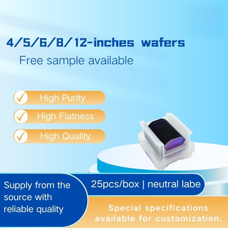
| Wafer Size | Diameter(mm) | Standard Thickness(μm) | Wafer Thickness Type | Material Category | Conduction Type | Crystal Growth Type | Processing Technology | Product Grade | Main Application Fields |
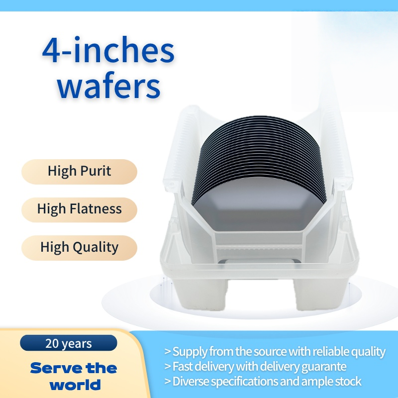
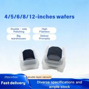
| 4 inch | 100 | 525 | Standard Thickness 500~775μm | Monocrystalline Silicon | P-type dominant, small amount of N-type | CN, FN, NTD | Single-sided polish / Double-sided polish / Etching / Single-sided polish + Etching | Prime Wafer / Test Wafer / Scrap Wafer | Transistors, MOSFET, TVS, sensors, miniature photovoltaic products, laboratory samples |
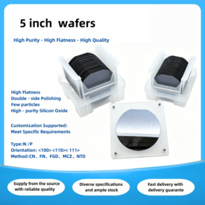
| 5 inch | 125 | 550 | Standard Thickness | Monocrystalline Silicon | P-type dominant, small amount of N-type | CN, FN | Single-sided polish / Double-sided polish / Etching | Prime Wafer / Test Wafer | Legacy power devices, traditional power supplies, simple photovoltaic modules, security equipment |
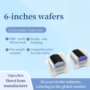
| 6 inch | 150 | 675 | Standard Thickness | Monocrystalline Silicon | P-type dominant, small amount of N-type | CN, FN, FGD, NTD | Single-sided polish / Double-sided polish / Etching, premium double-sided polish | Prime Wafer / Test Wafer | Power MOSFET, thyristors, Schottky diodes, mini on-board devices, household photovoltaic grid-connected parts |
| 8 inch | 200 | 725 | Standard / Thin Wafer | Monocrystalline Silicon | Both P-type & N-type available | FN, FGD, MCZ | Double-sided polish, Etching (core processes) | Prime Wafer | Power management IC, MCU, vehicle control units, large-scale photovoltaic power station modules |
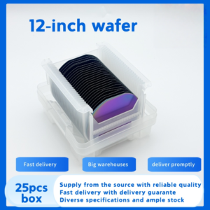
| 12 inch | 300 | 775 | Standard / Ultra-thin Wafer | Monocrystalline Silicon | Both P-type & N-type available | MCZ-dominant | Composite process of double-sided polish & etching, double-sided polish | Prime Wafer | CPU/GPU, memory & AI chips, premium automotive driver ICs |
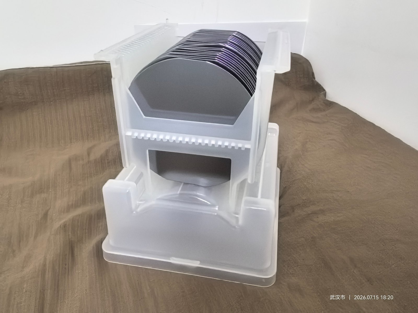
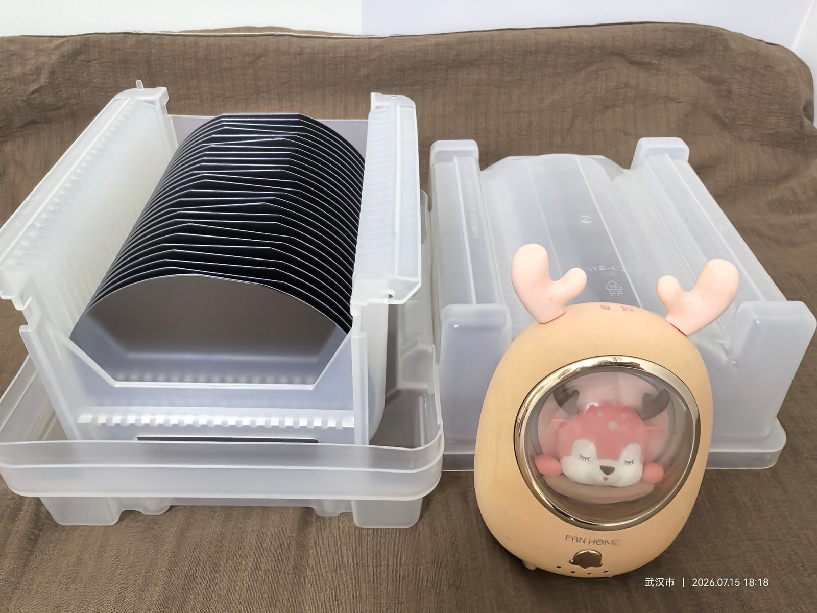
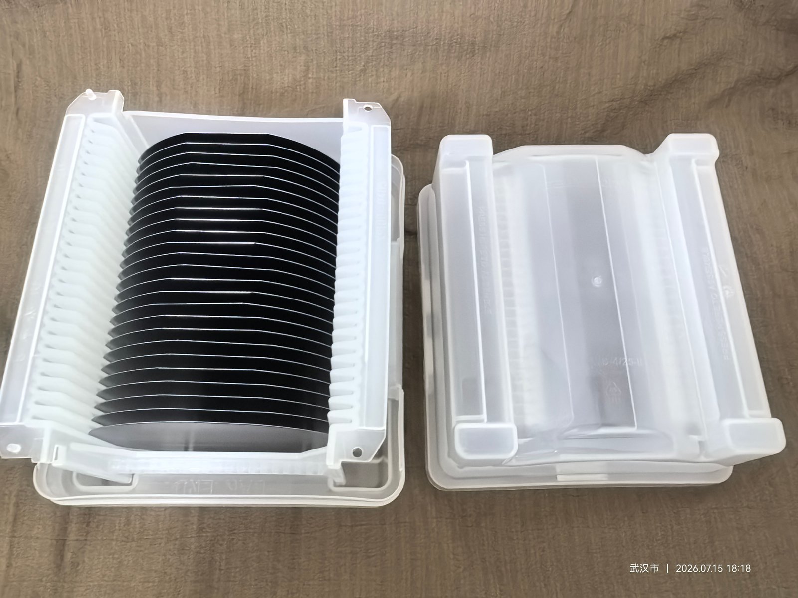
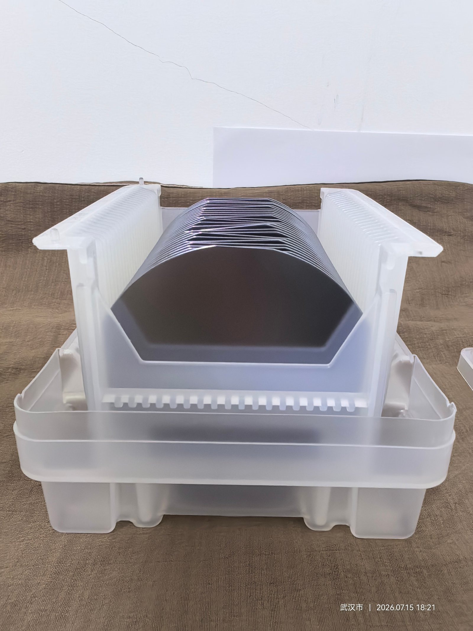
4-Inch Monocrystalline Silicon Wafer Product Description
Our 4-inch monocrystalline silicon wafers are produced via Czochralski (CZ) or Float-Zone (FZ) single crystal growth technology, featuring semiconductor-grade ultra-high purity from 9N to 11N. Available crystal orientations include <100> and <111>, with customizable P-type and N-type doping covering full resistivity ranges.
We provide multiple surface treatments: single-side polishing, double-side mirror polishing, and combined grinding & chemical etching. Strictly controlled thickness tolerance, TTV and warp deliver oxide-free ultra-clean surfaces with low defect density, high carrier mobility, stable conductivity and minimal leakage current.
Compatible with legacy small-scale semiconductor production lines, university labs, LED chips, power devices, MEMS sensors, mini PV modules, miniature automotive electronics, as well as photolithography, thin-film deposition, ion implantation and other core processes.
Boasting high mechanical hardness and low thermal expansion coefficient, the wafers resist deformation and cracking under high-temperature processing. Ultra-low impurity content guarantees consistent electrical performance across batches. Factory direct supply with abundant stock; customized thickness, doping and surface processes are available. Cost-effective for medium & small wafer manufacturers, research labs and bulk foreign trade shipments.