| 类别(中文) | 参数(中文) | 详情(中文) | Category (English) | Parameter (English) | Details (English) |
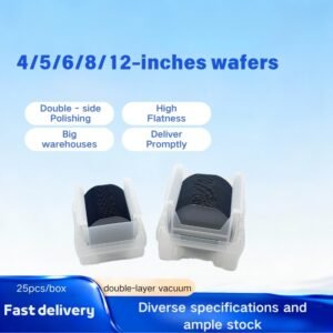
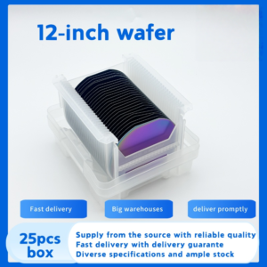
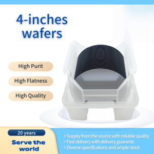
| 基本参数 | 尺寸 | 6英寸(150mm) | Basic Parameters | Size | 6 inch (150mm) |
| 基本参数 | 纯度 | 半导体级 9N~11N | Basic Parameters | Purity | Semiconductor Grade 9N~11N |
| 基本参数 | 晶体生长工艺 | 直拉法(CZ) / 区熔法(FZ);NTD中子嬗变掺杂可选 | Basic Parameters | Crystal Growth Process | Czochralski (CZ) / Float-Zone (FZ); NTD doping optional |
| 基本参数 | 晶向 | <100> / <111>(可定制) | Basic Parameters | Crystal Orientation | <100> / <111> (customizable) |
| 电气性能 | 导电类型 | P型 / N型(可定制) | Electrical Performance | Conductivity Type | P-type / N-type (customizable) |
| 电气性能 | 电阻率 | 0.001~10000Ω·cm 可控,均匀性好,偏差小 | Electrical Performance | Resistivity | 0.001~10000Ω·cm controllable, good uniformity, minimal deviation |
| 表面与物理特性 | 表面工艺 | 单面抛光(SSP)、双面镜面抛光(DSP)、双磨+化腐、研磨+化学腐蚀 | Surface & Physical Properties | Surface Process | Single-side Polishing (SSP), Double-side Mirror Polishing (DSP), Double Grinding & Etching, Grinding & Chemical Etching |
| 表面与物理特性 | 厚度 | 675μm / 725μm 常规,薄型/超薄型可定制 | Surface & Physical Properties | Thickness | 675μm / 725μm standard, thin/ultra-thin customizable |
| 表面与物理特性 | 表面质量 | 无氧化层、无划痕、高平整度、低粗糙度、低缺陷密度、亲水性好 | Surface & Physical Properties | Surface Quality | Oxide-free, scratch-free, high flatness, low roughness, low defect density, good hydrophilicity |
| 机械与热性能 | 综合性能 | 机械强度高、抗震动、热稳定性好、耐高低温、耐腐蚀、抗热冲击 | Mechanical & Thermal Properties | Comprehensive Properties | High mechanical strength, vibration resistance, excellent thermal stability, wide temperature tolerance, corrosion resistance, thermal shock resistance |
| 核心优势 | 性能特点 | 晶界少、导电性能优、批次稳定性强、良率高、平整度佳、薄膜沉积效果好 | Key Advantages | Performance Features | Few grain boundaries, excellent conductivity, strong batch consistency, high yield, superior flatness, ideal for thin film deposition |
| 应用领域 | 核心应用 | 功率半导体、二三极管制造、传感器、光伏逆变器、汽车电子、整车电控 | Application Fields | Core Applications | Power semiconductors, diode & triode manufacturing, sensors, PV inverters, automotive electronics, vehicle electronic control |
| 应用领域 | 其他应用 | 集成电路、化工电子、丝网印刷工艺、芯片制程、安防器件、可控硅 | Application Fields | Other Applications | Integrated circuits, chemical electronics, screen printing process, chip manufacturing, security devices, thyristors |
| 交付与服务 | 现货状态 | 常规型号现货充足,正片/试片可选 | Delivery & Service | Stock Status | Ample stock for standard models, prime/test wafers optional |
| 交付与服务 | 定制服务 | 支持厚度、电阻率、掺杂类型、表面工艺、包装全维度定制 | Delivery & Service | Customization | Full customization support for thickness, resistivity, doping type, surface process, packaging |
| 交付与服务 | 交付优势 | 工厂直供价、品质统一、环保材质达标、外贸快速发货 | Delivery & Service | Delivery | Factory-direct pricing, consistent quality, eco-friendly material compliant, fast foreign trade shipment |
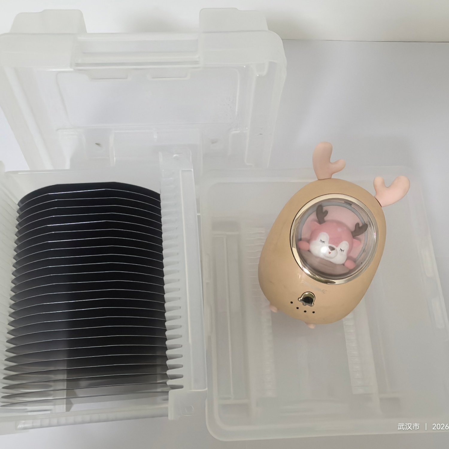
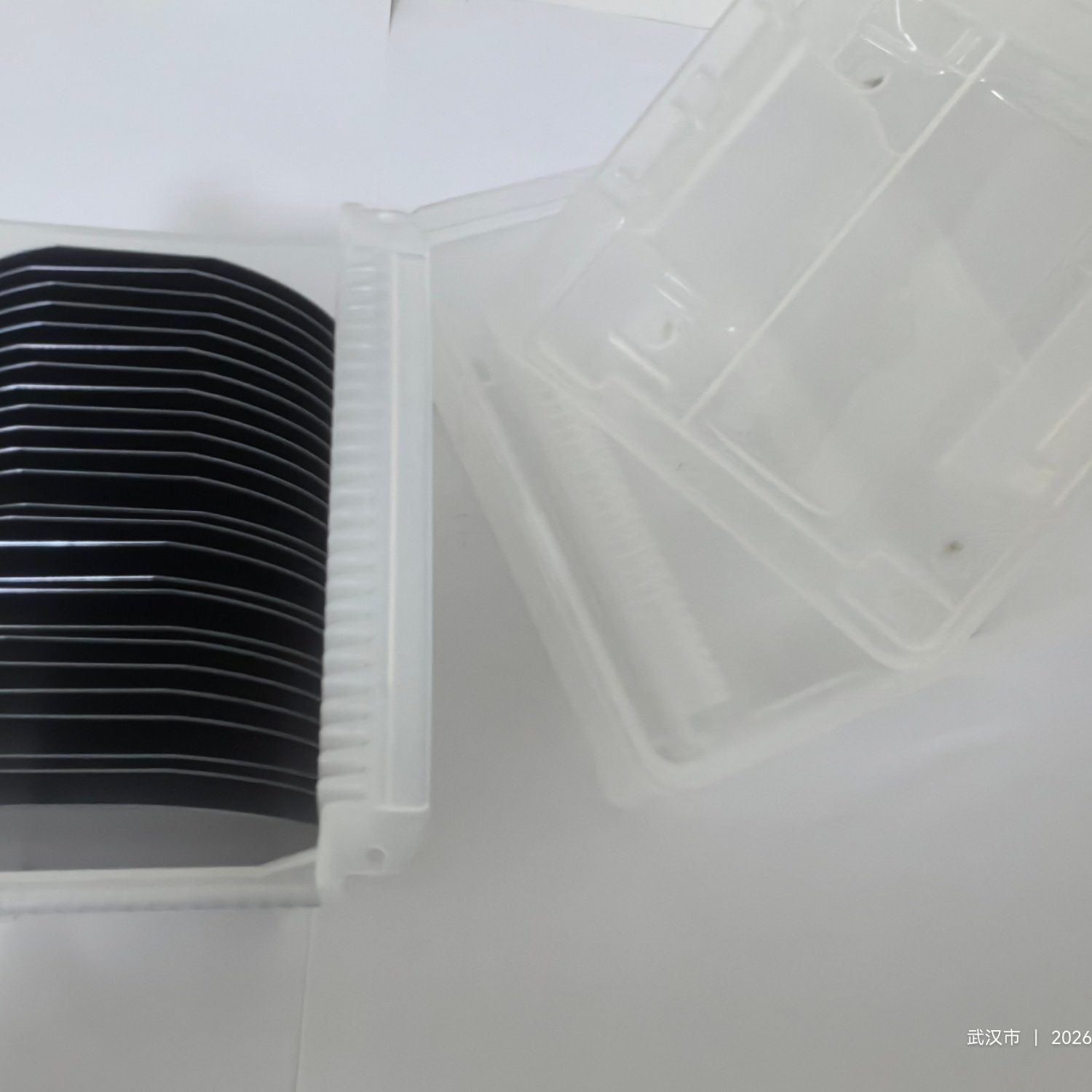
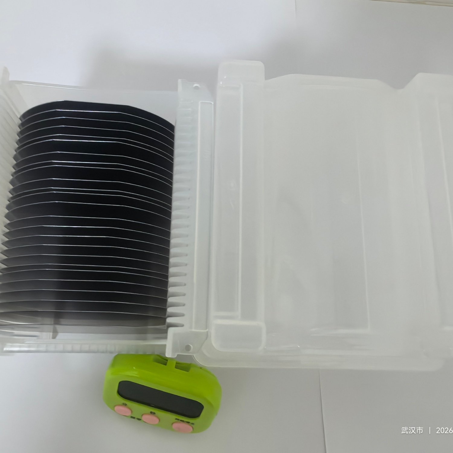
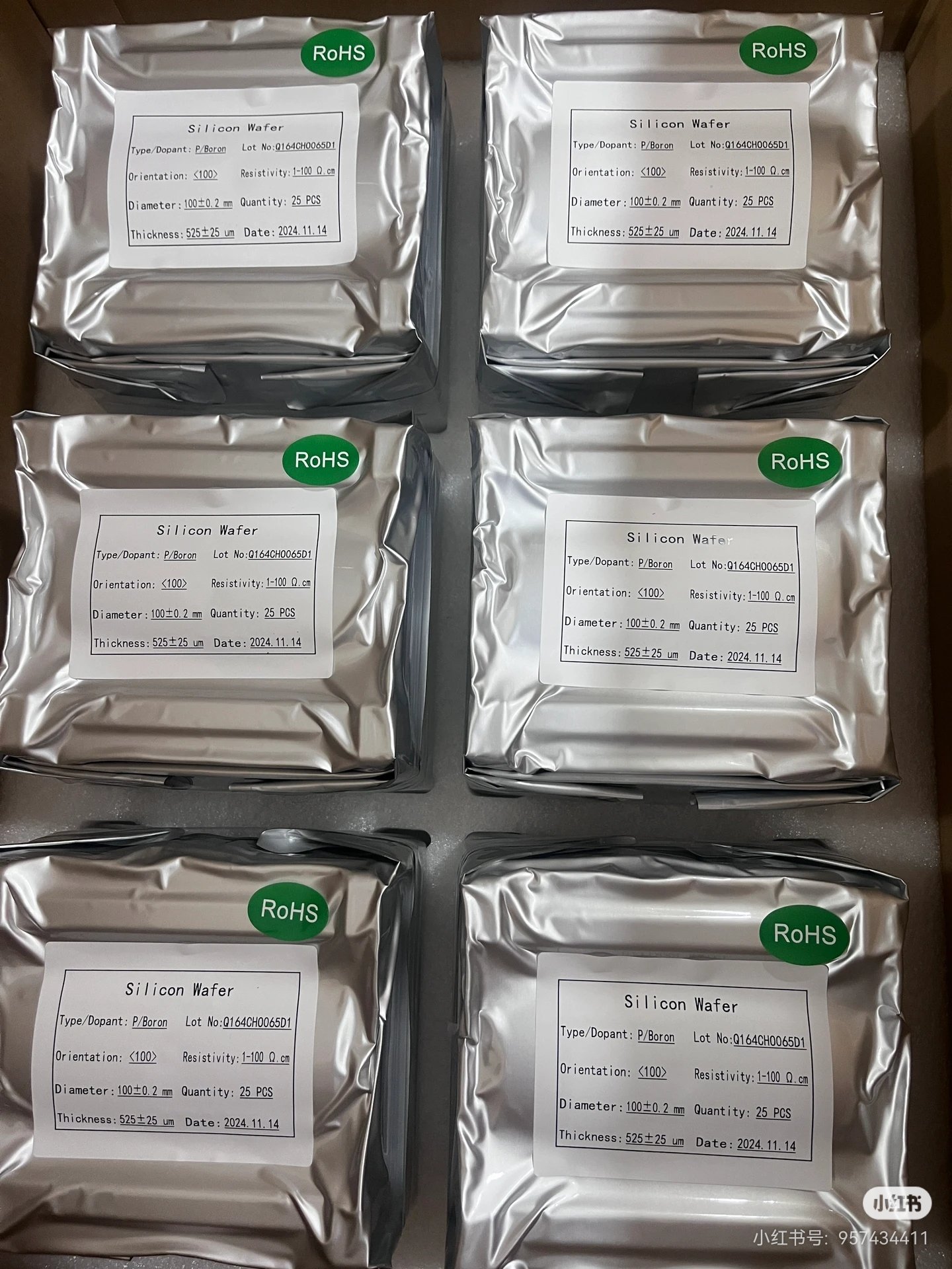
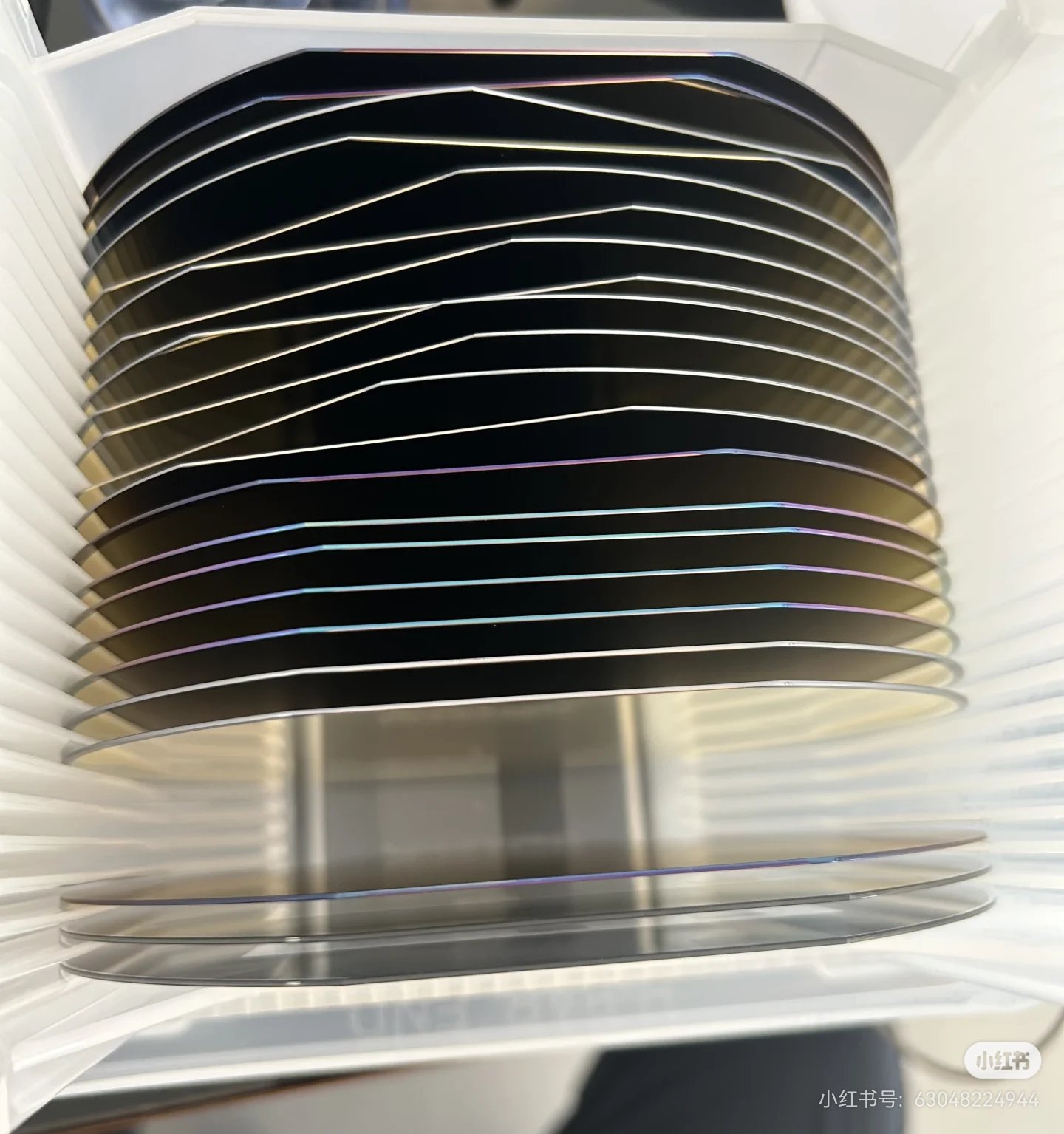
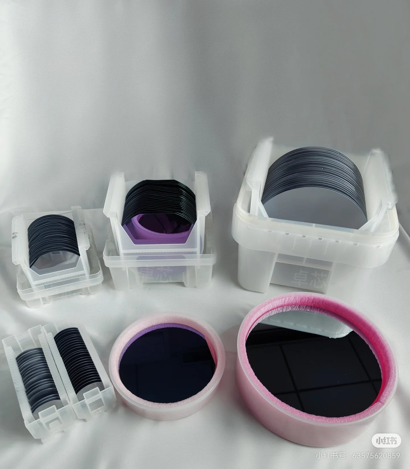
 5-inch polycrystalline silicon wafers with qualified crystal pulling purity, competitive factory pricing & fast delivery
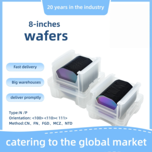 8-inch silicon wafers with high precision, abundant inventory, compatible with equipment assembly large stock
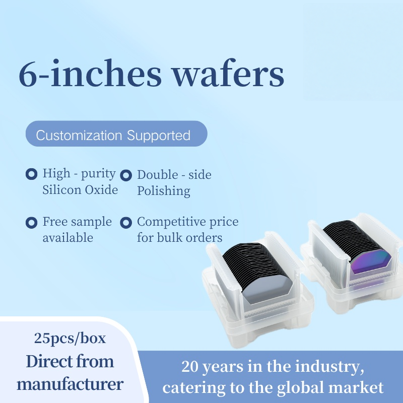
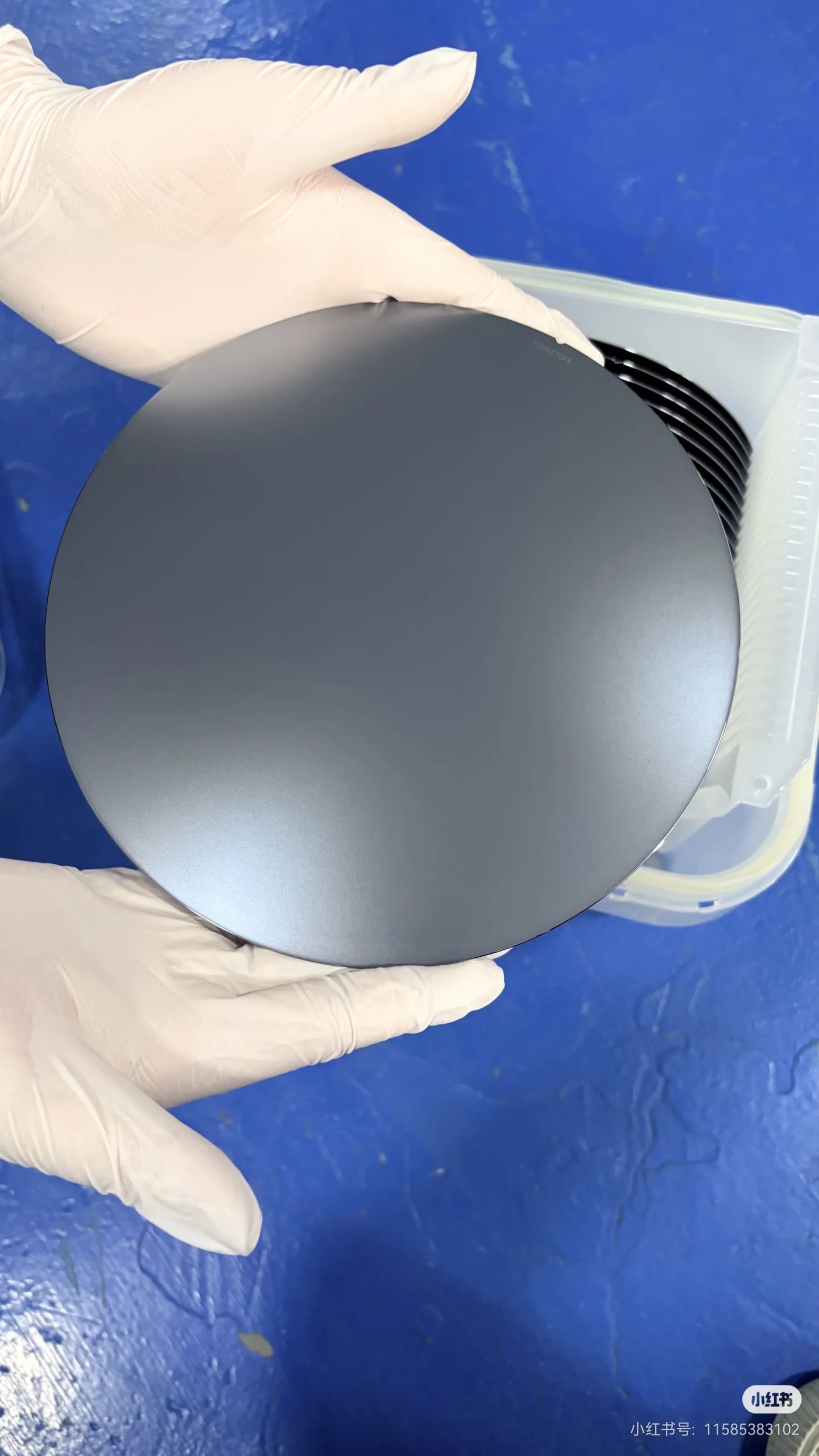
Factory Direct 6 Inch Silicon Wafer Competitive Price Fast Delivery outstanding thermal stability, high purity for high & low temperature environments, durable for outdoor use
| Product Specification Description | |
| Size | 4inch/5inch/6inch/7inch/12inch |
| Diameter (mm) | 100mm/125mm/150mm/200mm/300mm/ |
| Thickness (μm) | Conventional: 500 – 775μm; Thin wafers: 150 – 200μm; Ultra – thin: 10 – 50μm |
| Orientation | <100> <110>< 111> |
| Growth Method | CN、FN、FGD、MCZ、NTD |
| Surface conditions | grinding (single – side/double – side) chemical etching polishing (single-side/doubl-side) |
| Type | N /P |
| Dopant | N:(P)、(As)、(Sb) P:(B) |
| Resistivity (Ω·cm) | Low resistance / heavy doping: 0.001 – 0.1 Medium resistance: 0.1 – 100 High resistance: 100 – 1000 Ultra – high resistance: > 1000 |
| Purity | Semiconductor – grade: 9N – 11N Photovoltaic – grade: 6N |