| 类别(中文) | 参数(中文) | 详情(中文) | Category (English) | Parameter (English) | Details (English) |
| 基本参数 | 尺寸 | 12英寸(300mm) | Basic Parameters | Size | 12 inch (300mm) |
| 基本参数 | 纯度 | 半导体级 9N~11N,低氧含量高纯度 | Basic Parameters | Purity | Semiconductor Grade 9N~11N, low oxygen content, ultra-high purity |
| 基本参数 | 晶体生长工艺 | 直拉法(CZ) / 区熔法(FZ),单/多晶可选 | Basic Parameters | Crystal Growth Process | Czochralski (CZ) / Float-Zone (FZ), mono/polycrystalline optional |
| 基本参数 | 晶向 | <100> / <111>(可定制) | Basic Parameters | Crystal Orientation | <100> / <111> (customizable) |
| 电气性能 | 导电类型 | P型 / N型 可定制,电阻率可控 | Electrical Performance | Conductivity Type | P-type / N-type customizable, controllable resistivity |
| 电气性能 | 电阻率 | 高精度均匀分布,整片一致性强,满足个性化需求 | Electrical Performance | Resistivity | High-precision uniform distribution, excellent wafer-to-wafer consistency, meets personalized requirements |
| 表面与物理特性 | 表面工艺 | 双面镜面抛光、化腐工艺、边缘去毛刺、真空封装兼容、激光加工兼容 | Surface & Physical Properties | Surface Process | Double-side mirror polishing, chemical etching, burr-free edge, vacuum packaging compatible, laser processing compatible |
| 表面与物理特性 | 厚度 | 775μm 标准,常规/薄/超薄可选,厚度可定制 | Surface & Physical Properties | Thickness | 775μm standard, standard/thin/ultra-thin options, customizable thickness |
| 表面与物理特性 | 表面质量 | 无裂纹气泡、无划痕、表面洁净达标、抗氧化、性能不衰减 | Surface & Physical Properties | Surface Quality | Crack & bubble-free, scratch-free, clean surface compliant, anti-oxidation, non-degrading performance |
| 机械与热性能 | 综合性能 | 耐腐蚀、热导率适中、散热优异、晶体质密、机械性能稳定、抗老化 | Mechanical & Thermal Properties | Comprehensive Properties | Corrosion resistant, moderate thermal conductivity, excellent heat dissipation, dense crystal lattice, stable mechanical performance, anti-aging |
| 核心优势 | 性能特点 | 边缘无毛刺加工安全、适配自动化产线、综合性价比高、可靠性强、寿命长 | Key Advantages | Performance Features | Burr-free edges for safe machining, compatible with automated production lines, high cost-performance, high reliability, long service life |
| 应用领域 | 核心应用 | AI芯片、航天电子、传感器制造、高端晶圆制造、电源IC、头部晶圆厂 | Application Fields | Core Applications | AI chips, aerospace electronics, sensor manufacturing, high-end wafer fabrication, power ICs, leading wafer fabs |
| 应用领域 | 其他应用 | 新能源汽车车载设备、实验室研发、封装测试一体化、老产线升级、外贸出口 | Application Fields | Other Applications | NEV on-board equipment, laboratory R&D, integrated packaging & testing, legacy production line upgrades, foreign trade export |
| 交付与服务 | 现货状态 | 各型号齐全,现货充足,适配批量订单需求 | Delivery & Service | Stock Status | Full model range, ample stock, suitable for bulk order demands |
| 交付与服务 | 定制服务 | P/N型、厚度、电阻率、表面工艺、包装全维度可定制 | Delivery & Service | Customization | Full customization: P/N type, thickness, resistivity, surface process, packaging |
| 交付与服务 | 交付优势 | 工厂直供价、包装防护好、适配外贸长途快速发货、降低采购成本 | Delivery & Service | Delivery | Factory-direct pricing, well-protected packaging, suitable for long-distance foreign trade fast shipment, reduces procurement costs |
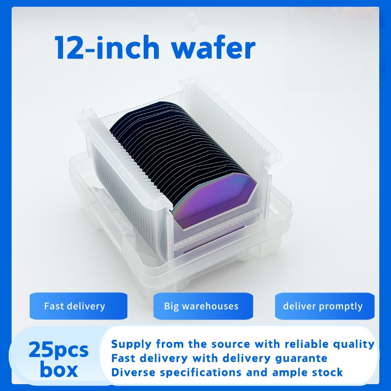
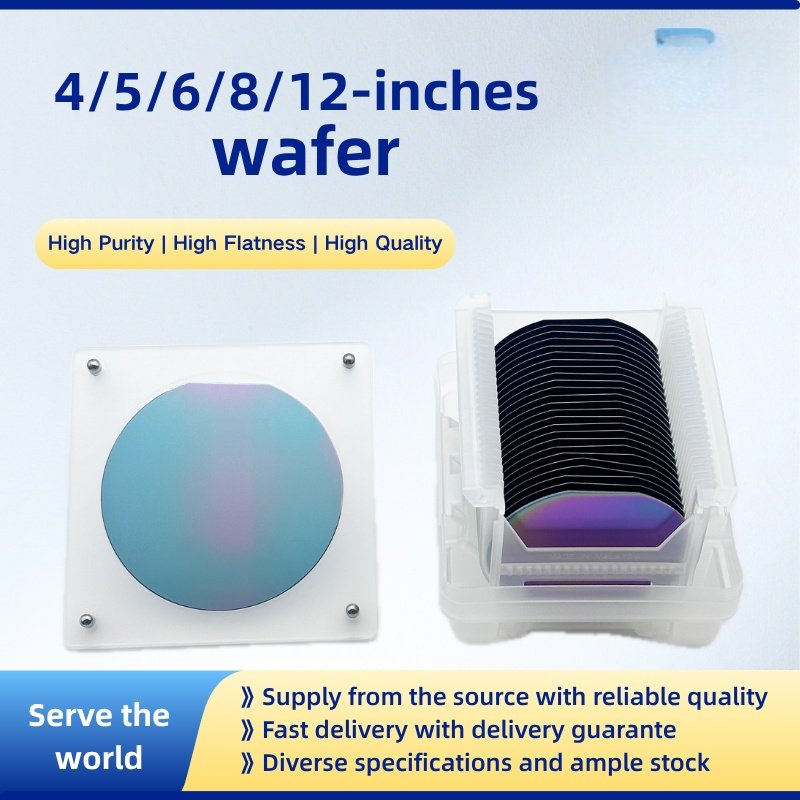
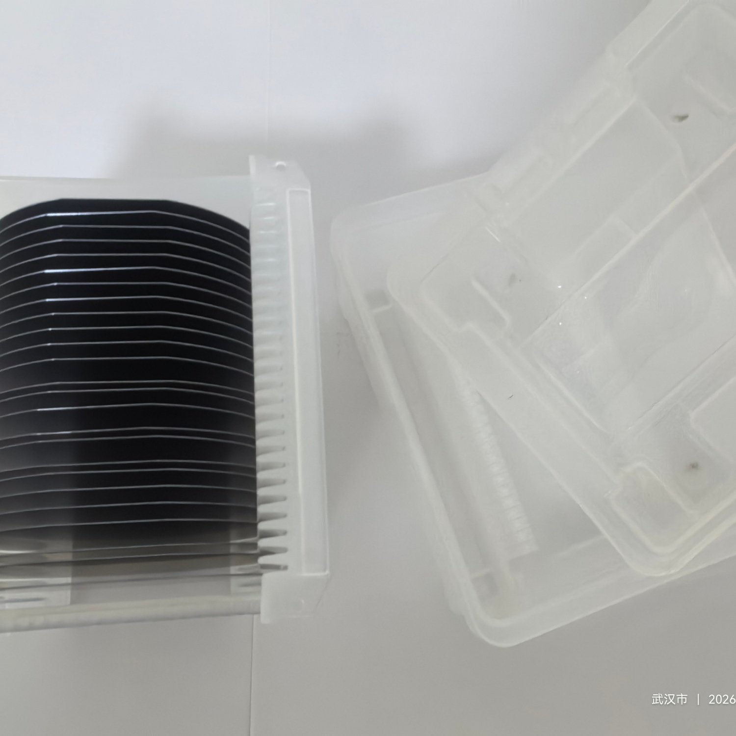
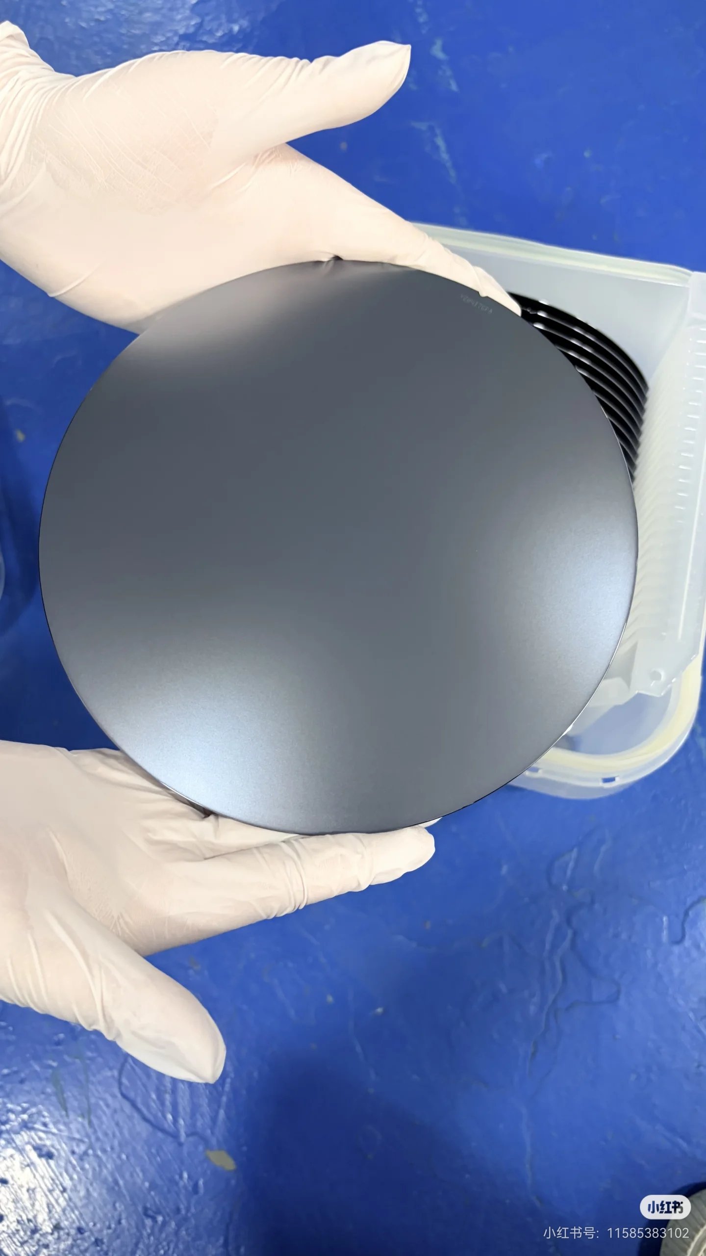
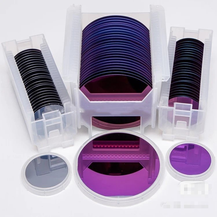
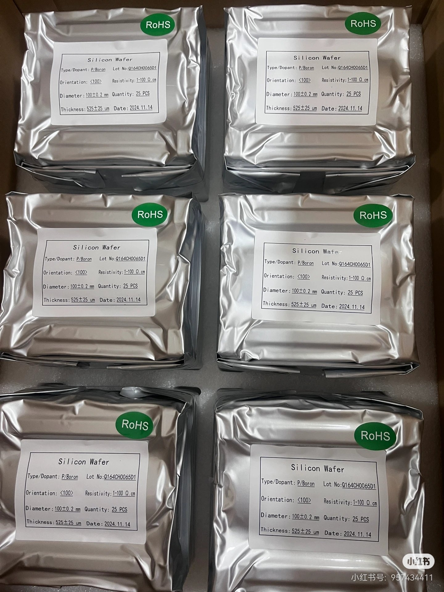
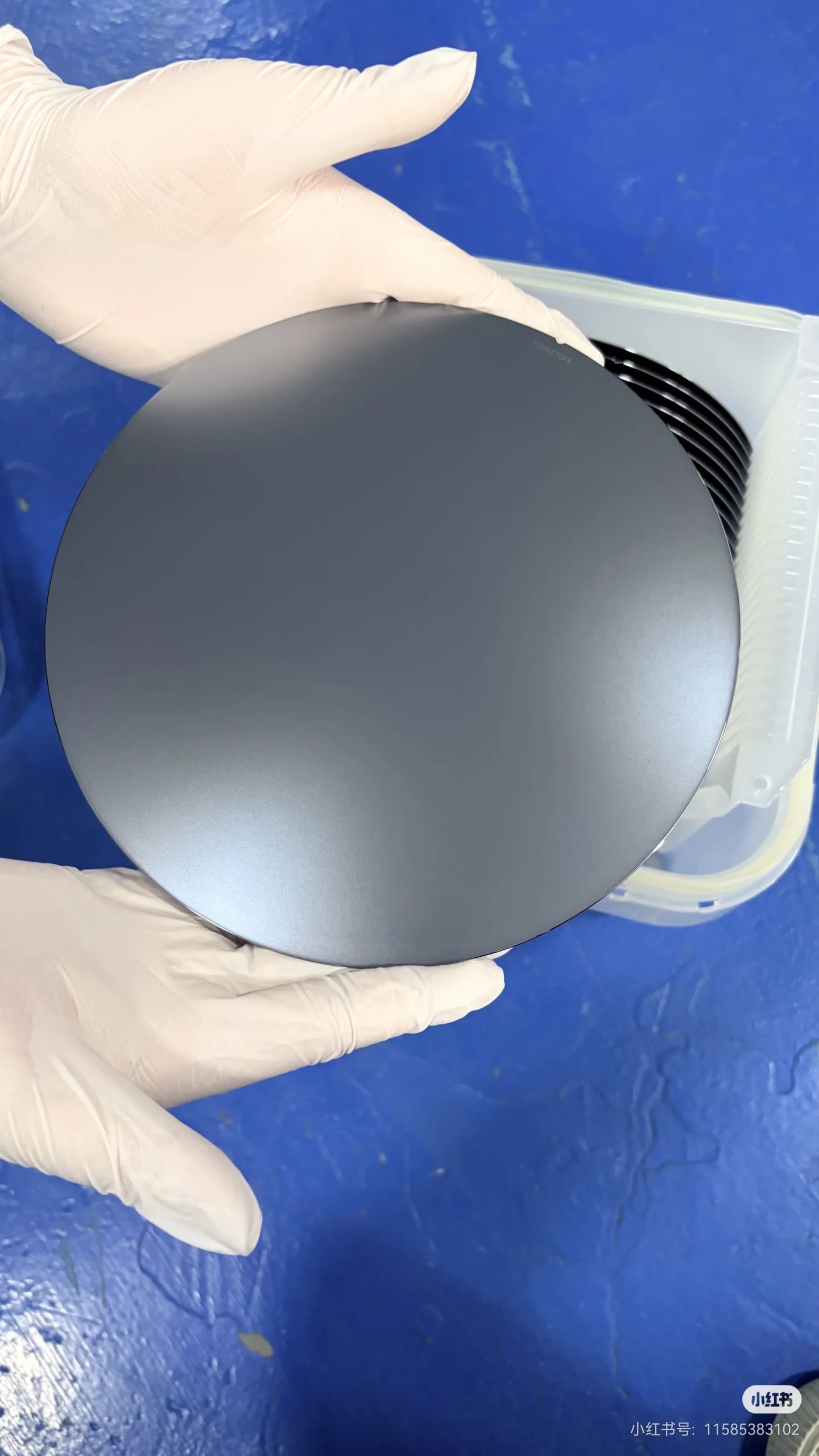
High-purity 12-inch silicon wafers for electronic components, mainly P-type, stable operation, ample stock
| Product Specification Description | |
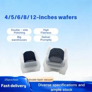
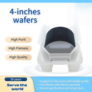
| Size | 4inch/5inch/6inch/8inch/12inch |
| Diameter (mm) | 100mm/125mm/150mm/200mm/300mm/ |
| Thickness (μm) | Conventional: 500 – 775μm; Thin wafers: 150 – 200μm; Ultra – thin: 10 – 50μm |
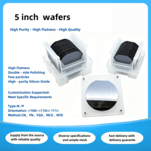
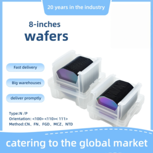
| Orientation | <100> <110>< 111> |
| Growth Method | CN、FN、FGD、MCZ、NTD |
| Surface conditions | grinding (single – side/double – side) chemical etching polishing (single-side/doubl-side) |
| Type | N /P |
| Dopant | N:(P)、(As)、(Sb) P:(B) |
| Resistivity (Ω·cm) | Low resistance / heavy doping: 0.001 – 0.1 Medium resistance: 0.1 – 100 High resistance: 100 – 1000 Ultra – high resistance: > 1000 |
| Purity | Semiconductor – grade: 9N – 11N Photovoltaic – grade: 6N |